I am Anirudha Behera, a diligent Graduate student at Illinois Institute of Technology, Chicago, specializing in Electrical Engineering with a concentration in Computers and Microelectronics. My education includes advanced coursework in VLSI, CAD techniques, and high-performance IC systems, underpinning my expertise as a Certified VLSI Physical Design Engineer. In the professional realm, I have demonstrated extensive proficiency in ASIC design, particularly mastering the RTL to GDSII flow. My experience is supported by my adept use of industry-leading EDA tools including Synopsys, Cadence, Mentor Graphics, and Xilinx, which has driven exceptional outcomes in both academic and project settings. Through hands-on roles, such as a Research Assistant at IIT’s Design Automation Lab and a Physical Design Intern at Chipedge Technology, I have effectively utilized FPGA boards and contributed to research projects on ASIC and FPGA development. My projects have involved pioneering techniques for optimizing design quality and efficiency, particularly for advanced technology nodes. Currently, I am seeking an entry-level position where I can leverage my technical skills, contribute to innovative projects, and continue my professional development within a dynamic engineering team.
Standard Cell-Based ASIC Design for 8-bit Accumulator
Implemented Verilog code and Testbench for the 8-bit Accumulator, then synthesized the RTL codes. Executed Logical Synthesis process using DC tool, and recorded area, power, and timing reports. Performed PnR using Encounter. After PnR buffers are added and then performed Post PnR and recorded optimized area, power, and timing results, and performed Formal verification. Collected GDSII file and plotted the final Layout. .

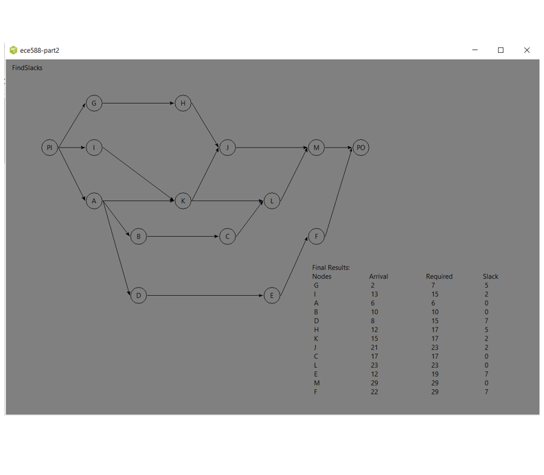
CAD Tool Design for Static Timing Analysis by using Tcl/Tk and C
Designed C code to calculate the required time, arrival time, and slack time from the given input matrix file and save the output file separately. Designed a Static Timing Analysis CAD tool GUI using TCL/Tk, which can take inputs from the user and optimize the given input matrix using implemented C code and display the output results on the GUI interface. .
Hierarchical Schematic and Layout Design of 4-bit Carry Look-ahead Adder
Designed a 4-bit CLA adder schematic, Symbol, Testing Circuit, and Layout using Virtuoso. Performed LVS, DRC, and PEX using MG Calibre. Then Formal verification is performed using Formality. Measured Power, Delay, and temperature using HSPICE. .


