Anirudha Behera
Very Large-Scale Integration Engineer
Standard Cell-Based ASIC Design for 8-bit Accumulator
Implemented Verilog code and Testbench for the 8-bit Accumulator, then synthesized the RTL codes. Executed Logical Synthesis process using DC tool, and recorded area, power, and timing reports. Performed PnR using Encounter. After PnR buffers are added and then performed Post PnR and recorded optimized area, power, and timing results, and performed Formal verification. Collected GDSII file and plotted the final Layout.
CAD Tool Design for Static Timing Analysis by using Tcl/Tk and C
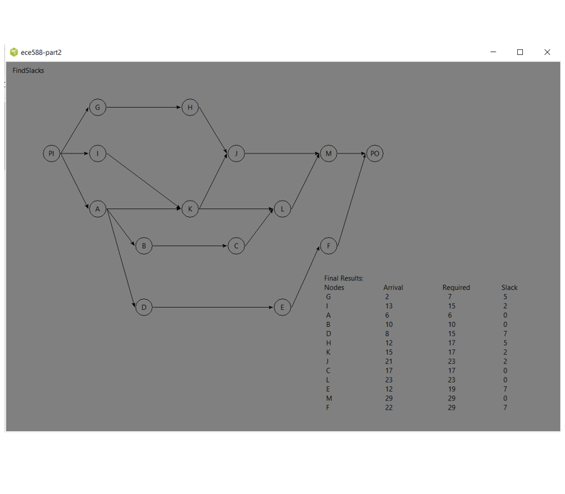
Designed C code to calculate the required time, arrival time, and slack time from the given input matrix file and save the output file separately. Designed a Static Timing Analysis CAD tool GUI using TCL/Tk, which can take inputs from the user and optimize the given input matrix using implemented C code and display the output results on the GUI interface.
Hierarchical Schematic and Layout Design of 4-bit Carry Look-ahead Adder
Designed a 4-bit CLA adder schematic, Symbol, Testing Circuit, and Layout using Virtuoso. Performed LVS, DRC, and PEX using MG Calibre. Then Formal verification is performed using Formality. Measured Power, Delay, and temperature using HSPICE.

1-Bit Ripple Carry Adder Schematic Design and Testing
I draw the adder schematic using Virtuoso to perform binary addition operation of two bits, which are a and b with an input carry (ci). The delay measurements were performed, and they are found to be as expected value. Then we verified the SPICE netlist against the Verilog module (adder.v) to test the functionalities of the proposed adder. After successfully running ESP, I found to match (passed) and hence the functionalities of the adder were successfully verified.
Design & Implementation of Gate Level CAD Tool for 4-bit RCA
I implemented the code to achieve targeted GUI interface and hierarchical gate-level netlist view. I used 16-bit RCA, 8-bit RCA and 4-bit RCA modules for this CAD tool design. The final GUI interface is designed into a five-level hierarchy model which are top-level, first level, second level, third level and Leaf Level hierarchical view. The GUI interface was designed using TCL and the modules were designed using Verilog HDL..
32-bit Pipelined CPU Design with Modified New ALU Architecture
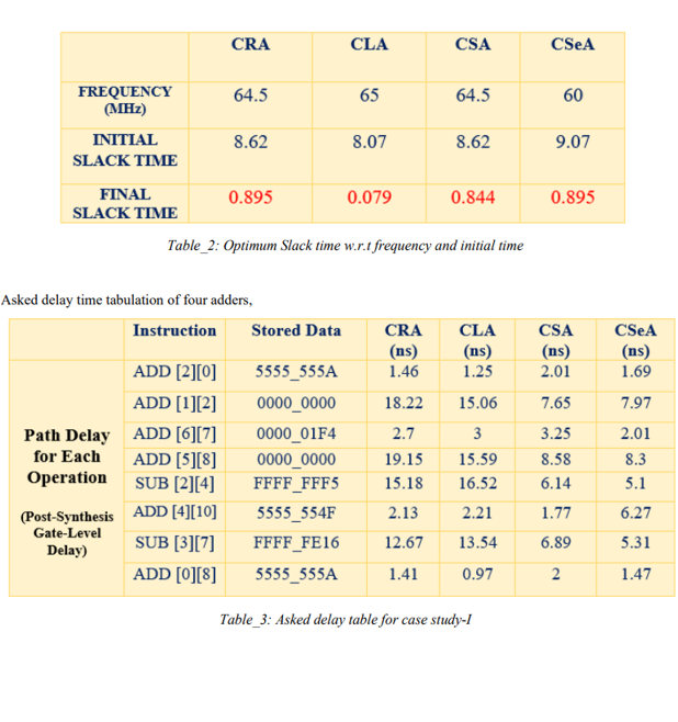
Implemented five different 32-bit CPU architectures using standard ASIC flow to achieve desired slack time. Four of them were using CRA, CLA, CSA, and CSeA Adders. The fifth one is with Comparator and CLA adder. Performed RTL Synthesis, Logic Synthesis, PnR, and Post PnR, for each design, and initial slack time and final optimized slack time were recorded with power and area reports. Finally, GDSII Layout files were collected.
System Level MMP Configuration for Ultra-low Power Optimization
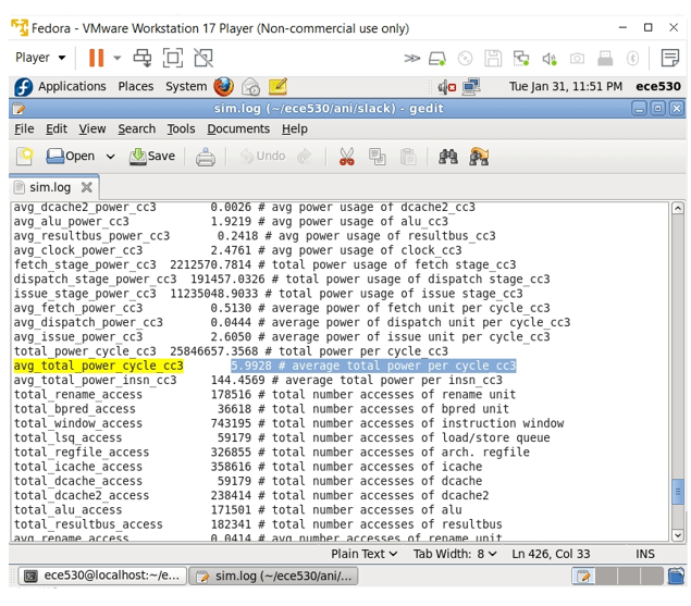
Designed C code for Graph-based slack time analysis method, then reduced the power consumption of the program using Loop unrolling techniques and measured the power using WATCH tool. To minimize further power, catch optimization technique is used and power measured using the CACTI tool. Total 85.68% power saving recorded.
Register Transfer Level MMP Configuration for Ultra-low Power Optimization
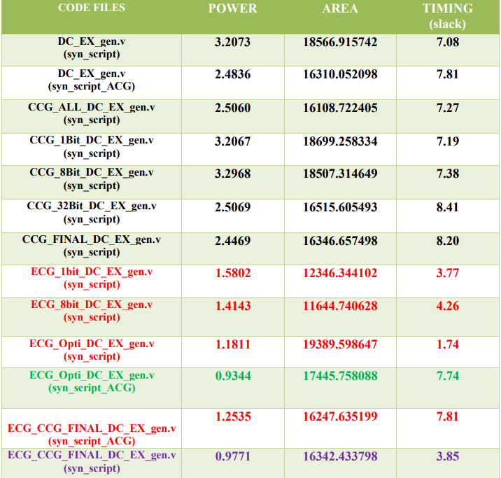
Implemented clock gating techniques like ACG, CCG, OCCG, ECG, LECG and hybrid techniques on a Mobile Multimedia Processor design (MMP) to reduce power consumption by modifying the RTL source code accordingly. With the help of ECG and ACG hybrid model I was able to optimize power up to 109.75%. Formality and ModelSim were used for equality check and synthesis then Power Compiler is used for power measurement.
32-bit MIPS-Lite Multicycle Processor
Designed a Behavioral Model of a 5-Stage RISC architecture-based Reduced version of the Multicycle MIPS processor using the Xilinx Vivado ML tool. Targeted ISAs were implemented in the Memory for execution then simulation, RTL Analysis, synthesis, and implementation was performed.
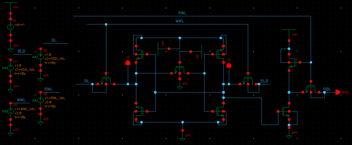
High Performance VLSI PVT-Aware Design for 10T SRAM using 15nm PDK
In order to prevent PVT Variation, I have proposed this 10T SRAM model. I used multiple techniques to optimize process, voltage, and temperature variation. Which are, three Bit Line method, multi VT technique, body Biasing technique and transistor Sizing technique. By using all these techniques and designe dy model and performed several transient analysis tests for both READ and WRITE operations. TA tests involve, Rising Propagation Delay, Falling Propagation Delay, Average Propagation Delay, Difference Between Delays, Rise Time, Fall Time, Dynamic Power, Static Power, Sub threshold leakage Current, Rush Current and Total Power.
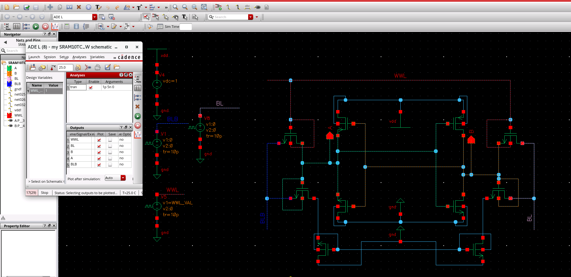
Fully Differential Cell Content Body Biased 10T SRAM Cell (CCBB10T)
This Variation resilient 10T SRAM model was proposed by Animul Islam, Mohd Hasan and Tughrul Arslan in 2012, International Journal of Electronics. This model is designed and Transient Analysis is performed in order to do comparition. The same TA tests were conducted for this model as well. Cadence Virtuoso is used for schematic design and HSPICE is used for netlist simulation. 15nm FinFET PDK tool kit is used to design this model.
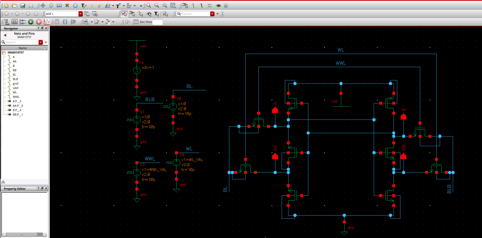
Schmitt trigger (ST) -based 10T SRAM bit cell
This Parameter Variation Tolerance and Error Resiliency: New Design Paradigm for the Nanoscale Era paper was published by Swaroop Ghosh and Kaushik Roy in 2010, IEEE Xplore. This model is designed and Transient Analysis is performed in order to do comparition. The same TA tests were conducted for this model as well. Cadence Virtuoso is used for schematic design and HSPICE is used for netlist simulation. 15nm FinFET PDK tool kit is used to design this model.